ASAHI KASEI
[AKD4562]
<KM061600>
'00/06
-
1
-
GENERAL DESCRIPTION
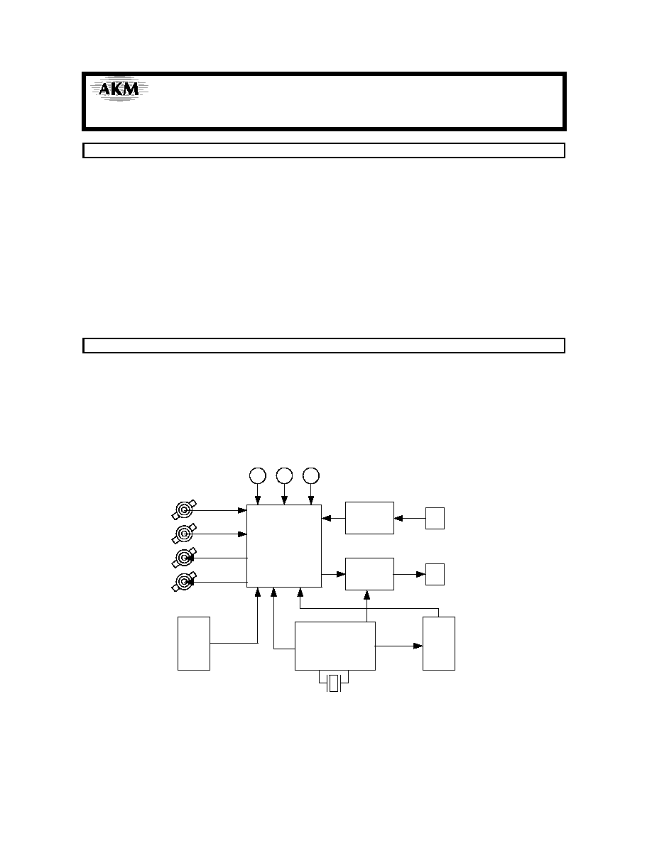
AKD4562 is an evaluation board for the portable digital audio 20bit A/D and D/A converter, AK4562. The
AKD4562 can evaluate A/D converter D/A converter separately in addition to loopback mode (A/D
D/A). The A/D section can be evaluated by interfacing with AKM's DAC evaluation boards directly. The
AKD4562 has the interface with AKM's wave generator using ROM data and AKM's ADC evaluation
boards. Therefore, it's easy to evaluate the D/A section. The AKD4562 also has the digital audio interface
and can achieve the interface with digital audio systems via opt-connector.
n
Ordering guide
AKD4562 --- Evaluation board for AK4562
(Cable
for
connecting
with
printer
port
of
IBM-AT,
compatible PC and control software are packed with this.)
FUNCTION
�
Compatible with 2 types of interface
- Direct interface with AKM's A/D & D/A converter evaluation boards
-
DIT/DIR
with
optical
input/output
�
BNC connector for an external clock input
�
10pin Header for serial control mode
LIN1/2
CS8412
(DIR)
AK4353
Clock
Generator
VT
VA GND
RIN1/2
LOUT1/2
ROUT1/2
AK4562
(DIT)
Opt Out
Opt In
10pin Header
A/D, D/A Data
ROM Data
Control
Data
10pin Header
Figure 1. AKD4562 Block Diagram
* Circuit diagram and PCB layout are attached at the end of this manual.
Evaluation board Rev.A for AK4562
AKD4562

ASAHI KASEI
[AKD4562]
<KM061600>
'00/06
-
2
-
1. Evaluation Board Manual
n
Input / Output circuits & Set-up jumper pin for Input / Output circuits
(1) LINE Block
(a) LIN1,2/RIN1,2 Input circuits
RIN1
RIN2
LIN2
LIN1
J2
LIN
R36
560
+
C38
10u
J4
RIN
R38
560
+
C41
10u
JP15
LIN
JP18
RIN
LIN1
LIN2
RIN1
RIN2
Figure 2. LIN1,2/RIN1,2 Input circuits
1. Analog signal is input to LIN1 and RIN1 pins via J2 and J4 connectors.
JP15
LIN
LIN2
LIN1
JP18
RIN
RIN2
RIN1
2. Analog signal is input to LIN2 and RIN2 pins via J2 and J4 connectors.
JP15
LIN
LIN2
LIN1
JP18
RIN
RIN2
RIN1
ASAHI KASEI
[AKD4562]
<KM061600>
'00/06
-
3
-
(b) LOUT1/ROUT1 and OPGAL/OPGAR Selection circuits
ROUT1
OPGAL
LOUT1
OPGAR
+
C39
1u
+
C37
22u
JP17
OPGL
R39
220
R34
220
+
C43
1u
J5
ROUT1
+
C40
1u
R35
10k
J3
LOUT1
R37
560
JP16
LIO
JP20
OPGR
JP19
RIO
+
C44
1u
R40
10k
+
C42
22u
R41
560
LOUT1
ROUT1
OPGL
OPGL
LOUT1
OPGR
OPGR
ROUT1
Figure 3. LOUT1/ROUT1 and OPGAL/OPGAR Selection circuits
1. Analog signal is input to OPGAL and OPGAR pins via J3 and J5 connectors.
JP19
RIO
JP17
OPGL
OPGR
ROUT1
OPGL
LOUT1
JP16
LIO
OPGL
LOUT1
JP20
OPGR
OPGR
ROUT1
2. Analog signal is output to LOUT1 and ROUT1 pins via J3 and J5 connectors.
JP19
RIO
JP17
OPGL
OPGR
ROUT1
OPGL
LOUT1
JP16
LIO
OPGL
LOUT1
JP20
OPGR
OPGR
ROUT1
3. Analog signal is input to OPGAL and OPGAR pins via LOUT1 and ROUT1 pins.
JP19
RIO
JP17
OPGL
OPGR
ROUT1
OPGL
LOUT1
JP16
LIO
OPGL
LOUT1
JP20
OPGR
OPGR
ROUT1

ASAHI KASEI
[AKD4562]
<KM061600>
'00/06
-
4
-
(2) Other Jumper pins
1. JP1 (CSN) : Selection of CSN pin
SSB
:
SSB
mode.
AKM :
AKM
mode.
2. JP2 (SSB) : Selection of SSB mode or AKM mode
OPEN :
AKM
mode.
SHORT
:
SSB
mode.
3. JP3 (TST) : Selection of TEST pin
OPEN :
Normal
mode.
SHORT
:
Test
mode.
*
Always
open.
4. JP4 (GND) : Analog ground and Digital ground
OPEN :
Separated.
SHORT : Common. (The connector "DGND" can be open.) <default>
5. JP5 (VT) : D2V and VT
OPEN :
Separated.
<default>
SHORT : Common. (The connector "VT" can be open.)
6. JP9 (SDTO) : SDTO of AK4562
Always open. It can be short for only evaluation mode "7)".
7. JP10 (MODE) : Setting mode of CS8412
OPEN :
I
2
S compatible mode.
SHORT
:
16
bit
LSB
justified.
* AKM assumes no responsibility for the trouble when using the above circuit examples.
n
Operation sequence
1) Set up the power supply lines.
[VA]
(orange)
=
2.2
3.0V : for VA of AK4562 (typ. 2.5V)
[VT]
(orange)
=
1.8
3.0V : for VT of AK4562 (typ. 2.5V)
[D2V]
(orange)
=
1.8
3.0V : for 74LVC541 (typ. 2.5V)
[D5V] (red)
=
3.6
5.0V : for logic (typ. 5.0V)
[AGND] (black)
=
0V
:
for
analog
ground
[DGND] (black)
=
0V
:
for
logic
ground
Each supply line should be distributed from the power supply unit.
VT and D2V must be same voltage level.
2) Set up the evaluation mode, jumper pins and DIP switches.
(See the followings.)
Note : This evaluation board corresponds to I
2
S compatible mode for evaluation of A/D.
3) Power on.
The AK4562 and AK4353 should be reset once bringing SW1, 2 "L" upon power-up.
ASAHI KASEI
[AKD4562]
<KM061600>
'00/06
-
5
-
n
Evaluation mode
Applicable Evaluation Mode
1) Evaluation of loopback mode (default)
2) Evaluation of D/A using ideal sine wave generated by ROM data
3) Evaluation of D/A using A/D converted data
4) Evaluation of D/A using DIR (Optical Link)
5) Evaluation of A/D using D/A converted data
6) Evaluation of A/D using DIT (Optical Link)
7) All interface signals including master clock are fed externally.
DIT
PORT1
PORT3
DIR
AKD53XX
A/D Board
ROM Board
AKD43XX
D/A Board
PORT4
AKD4562
1)
2)
3)
4)
5)
6)
CD Player
10pin-Header
10pin-Header
PORT2
1) Evaluation of loopback mode. <default>
Nothing should be connected to PORT3 and PORT4. In case of using external clock through a BNC
connector (J1), select EXT on JP13 (CLK) and short JP14 (XTE). This mode corresponds to only I
2
S
compatible mode.
JP13
CLK
JP12
DIR
JP6
X_BCLK
64fs
32fs
JP8
BCLK
JP14
XTE
JP7
LRCK
DIR
ADC
DIR
EXT
XTL
GND
VD
JP11
SDTI
DIR
ADC
DIR
ADC